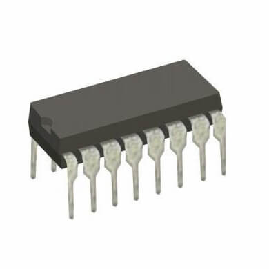
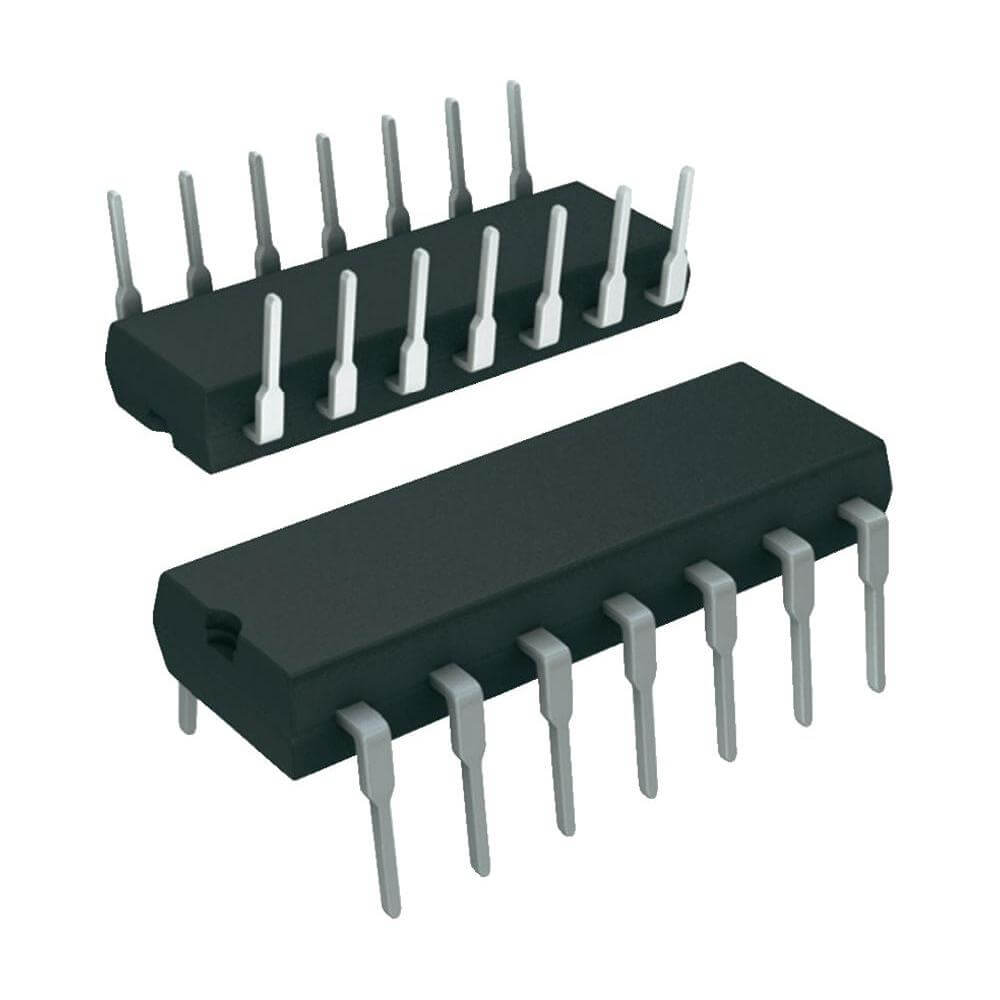
The 4011 is a quad 2-input NAND gate. The outputs are fully buffered for the highest noise immunity and pattern insensitivity to output impedance. It operates over a recommended VDD power supply range of 3 V to 15 V referenced to VSS (usually ground). Unused inputs must be connected to VDD, VSS, or another input.
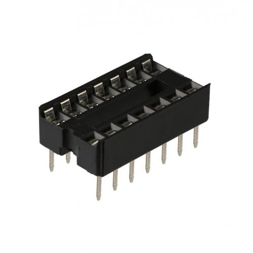
Pin description
| Symbol | Pin | Description |
| nA | 1, 5, 8, 12 | input |
| nB | 2, 6, 9, 13 | input |
| nY | 3, 4, 10, 11 | output |
| VSS | 7 | ground (0 V) |
| VDD | 14 | ?supply voltage |


Limiting values
| Symbol | Parameter | Conditions | Min | Max | Unit |
| VDD | supply voltage | ?0.5 | 18 | V | |
| IIK | input clamping current | VI < ?0.5 V or VI > VDD 0.5 V | ?10 | mA | |
| VI | input voltage | ?0.5 | VDD 0.5 | V | |
| IOK | output clamping current | VO < ?0.5 V or VO > VDD 0.5 V | ?10 | mA | |
| II/O | input/output current | ?10 | mA | ||
| IDD | supply current | 50 | mA | ||
| Tstg | storage temperature | ?65 | 150 | ?C | |
| Tamb | ambient temperature | ?40 | 125 | ?C | |
| Ptot | total power dissipation | Tamb = ?40 ?C to 125 ?C | |||
| SO14 | 500 | mW | |||
| P | power dissipation | per output | 100 | mW |
Download datasheet