وصف
CD4001B, CD4002B, and CD4025B NOR gates provide the system designer with direct implementation of the NOR function and supplement the existing family of CMOS gates. All inputs and outputs are buffered.
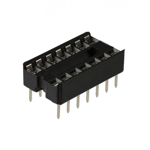
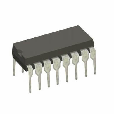
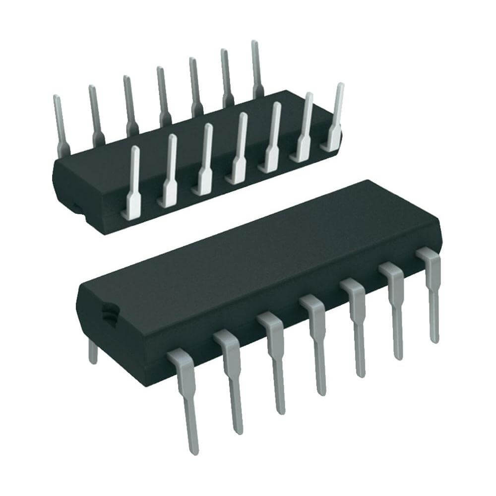
The CD4001B, CD4002B, and CD4025B types are supplied in 14-lead hermetic dual-in-line ceramic packages (F3A suffix), 14-lead dual-in-line plastic packages (E suffix), 14-lead small-outline packages (M, MT, M96, and NSR suffixes), and 14-lead thin shrink small-outline packages (PW and PWR suffixes).
The CD4001B, CD4002B, and CD4025B types are supplied in 14-lead hermetic dual-in-line ceramic packages (F3A suffix), 14-lead dual-in-line plastic packages (E suffix), 14-lead small-outline packages (M, MT, M96, and NSR suffixes), and 14-lead thin shrink small-outline packages (PW and PWR suffixes).
| PIN N? | SYMBOL | NAME AND FUNCTION |
| 1, 2, 5, 6, 8, 9, 12, 13 |
A, B, C, D, E, F, G, H |
Data Inputs |
| 3, 4, 10, 11 | J, K, L, M | Data Outputs |
| 7 | VSS | Negative Supply Voltage |
| 14 | VDD | Positive Supply Voltage |
VDD –> Supply Voltage –> (-0.5 to 22) V
VI –> DC Input Voltage –> (-0.5 to VDD 0.5) V
II –> DC Input Current –> (? 10) mA
PD –> Power Dissipation per Package –> (200) mW
–> Power Dissipation per Output Transistor –> (100) mW
Top –> Operating Temperature –> (-55 to 125) ?C
Tstg –> Storage Temperature –> (-65 to 150) ?C
سمات:
- Propagation delay time = 60 ns (typ.) at CL?= 50 pF, Vد?= 10 V
- Buffered inputs and outputs
- Standardized symmetrical output characteristics
- 100% tested for maximum quiescent current at 20 V
- تصنيفات بارامترية 5 فولت و10 فولت و15 فولت
- الحد الأقصى لتيار الإدخال هو 1 أمبير عند 18 فولت على نطاق درجة حرارة الحزمة الكاملة؛ 100 غ عند 18 فولت و25 درجة مئوية
- Noise margin (over full package temperature range):
1 V at Vد?= 5 V
2 V at Vد?= 10 V
2.5 V at Vد?= 15 فولت - يفي بجميع متطلبات معيار JEDEC المؤقت رقم 13ب، "المواصفات القياسية لوصف"ب؟ أجهزة سلسلة CMOS؟