

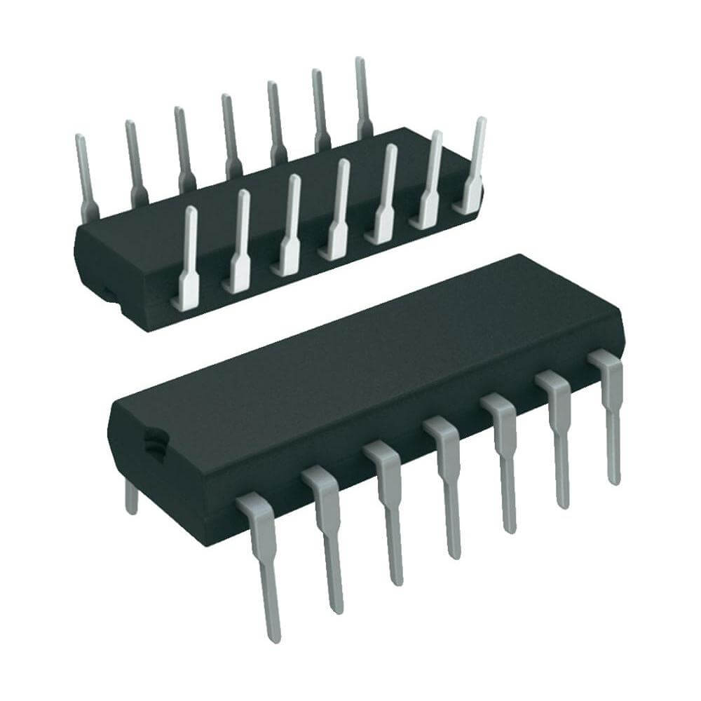
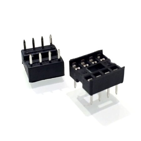
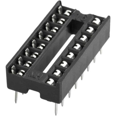
14 Pin IC Base IC Socket 7+7 Pin
Original price was: 3.00 EGP.2.00 EGPCurrent price is: 2.00 EGP.
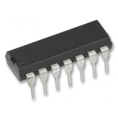
The 4066 device is a quad bilateral switch intended for the transmission or multiplexing of analog or digital signals. It is pin-for-pin compatible with the 4016 device, but exhibits a much lower on-state resistance.
The 4066 device is a quad bilateral switch intended for the transmission or multiplexing of analog or digital signals. It is pin-for-pin compatible with the 4016 device, but exhibits a much lower on-state resistance. In addition, the on-state resistance is relatively constant over the full signal input range.? The 4066 device consists of four bilateral switches, each with independent controls. Both the p and the n devices in a given switch are biased on or off simultaneously by the control signal. As shown in
the well of the n-channel device on each switch is tied to either the input (when the switch is on) or to VSS (when the switch is off). This
configuration eliminates the variation of the switch transistor threshold voltage with input signal and, thus, keeps the on-state resistance low over the full operating-signal range. The advantages over single-channel switches include peak input-signal voltage swings equal to the full supply voltage and more constant on-state impedance over the input-signal range. However, for sample-and-hold applications, the 4016 device is recommended.
Features
1? 15-V Digital or ?7.5-V Peak-to-Peak Switching
? 125-? Typical On-State Resistance for
15-V Operation
? Switch On-State Resistance Matched to Within
5 ? Over 15-V Signal-Input Range
? On-State Resistance Flat Over Full
Peak-to-Peak Signal Range
? High ON/OFF Output-Voltage Ratio:
80 dB Typical at fis = 10 kHz, RL = 1 k?
? High Degree of Linearity: <0.5% Distortion Typical
at fis = 1 kHz, Vis = 5 Vp-p
VDD ? VSS ? 10 V, RL = 10 k?
? Extremely Low Off-State Switch Leakage,
Resulting in Very Low Offset Current and High
Effective Off-State Resistance: 10 pA Typical at
VDD ? VSS = 10 V, TA = 25?C
? Extremely High Control Input Impedance
(Control Circuit Isolated From Signal Circuit):
1012 ? Typical
? Low Crosstalk Between Switches: ?50 dB Typical
at fis = 8 MHz, RL = 1 k?
? Matched Control-Input to Signal-Output
Capacitance: Reduces Output Signal Transients
? Frequency Response,
Switch On = 40 MHz Typical
? 100% Tested for Quiescent Current at 20 V
? 5-V, 10-V, and 15-V Parametric Ratings
Applications
? Analog Signal Switching/Multiplexing: Signal
Gating, Modulators, Squelch Controls,
Demodulators, Choppers, Commutating Switches
? Digital Signal Switching/Multiplexing
? Transmission-Gate Logic Implementation
? Analog-to-Digital and Digital-to-Analog
Conversions
? Digital Control of Frequency, Impedance, Phase,
and Analog-Signal Gain

Download Datasheet

Tell us what you are building and we will help you find suitable components, modules, development boards and tools from our available range.