

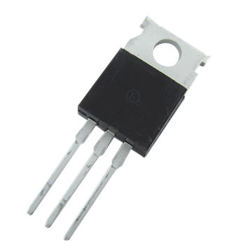
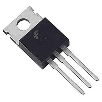
IRF540N N-Channel MOSFET TRANSISTOR 100V 0.044Ω 33A TO-220
Original price was: 25.00 EGP.18.00 EGPCurrent price is: 18.00 EGP.
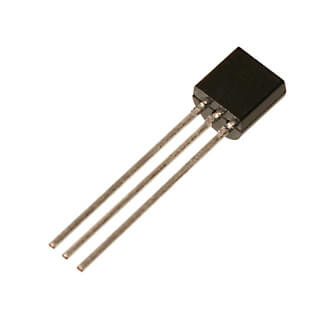
| Pin Number | Pin Name | Description |
| 1 | Emitter | Current Drains out through emitter, normally connected to ground |
| 2 | Base | Controls the biasing of transistor, Used to turn ON or OFF the transistor |
| 3 | Collector | Current flows in through collector, normally connected to load |
Note: Complete Technical Details can be found at the S8550 transistor datasheet given at the end of this article.
S8050
BC527, KSA708, MPS750
BC557, 2N3906, A1015, 2SA1943, BD140
S8550 is a PNP transistor hence the collector and emitter will be left open (Reverse biased) when the base pin is held at ground and will be closed (Forward biased) when a signal is provided to base pin. It has a maximum gain value of 300; this value determines the amplification capacity of the transistor normally S8550. Since it is very high it is normally used for amplification purposes.
When this transistor is fully biased then it can allow a maximum of 700mA to flow across the collector and emitter. This stage is called Saturation Region and the typical voltage allowed across the Collector-Emitter (VCE) or Collector-Base (VCB) could be 20V and 30V respectively. When base current is removed the transistor becomes fully off, this stage is called as the Cut-off Region.
As mentioned in the features the S8550 transistor is commonly used in push pull configuration with Class B amplifier. So let us discuss how that is done.
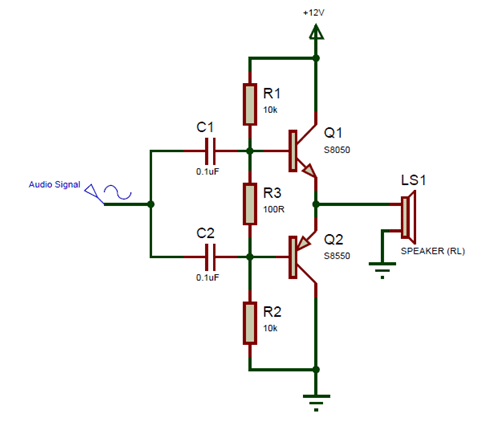
A push pull amplifier, commonly known as Class B amplifier is type of multistage amplifier commonly used for audio amplification of loudspeakers. It is very simple to construct and requires two identical complimentary transistors operate. By complimentary it means that we need a NPN transistor and its equivalent PNP transistor. Like here the NPN transistor will be S8050 and its equivalent PNP transistor will be S8550. A simple circuit diagram of the Class B amplifier with the using the S8050 is shown below.
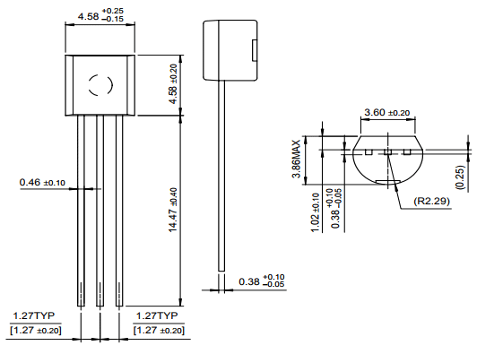
If you are designing a PCB or Perf board with this component then the following picture from the S8550 Datasheet will be useful to know its package type and dimensions.





Tell us what you are building and we will help you find suitable components, modules, development boards and tools from our available range.